Semiconductor Ceramics are a class of functional ceramic materials with unique electrical properties. Their conductivity lies between that of conductors and insulators and can be adjusted through compositional control, doping, or processing methods to exhibit semiconductor characteristics.
Semiconducting Mechanism:
Free charge carriers (electrons or holes) are introduced through doping (e.g., adding elements with different valence states into metal oxides) or defect engineering (such as creating oxygen vacancies).
Nonlinear Conductivity: For example, varistor ceramics (such as ZnO) show a sudden drop in resistance at a critical voltage, serving as overvoltage protection.
Temperature Sensitivity: Positive Temperature Coefficient (PTC) ceramics (such as BaTiO₃-based materials) exhibit a sharp increase in resistance with rising temperature, enabling self-regulating heating applications.
Combustible gas detection, environmental monitoring
Photosensitive Ceramics
CdS, CdSe
Photoconductive effect
Light-controlled switches, solar cells
2. Preparation Process
Raw Material Processing: High-purity oxide powders (e.g., ZnO, BaTiO₃) are mixed with dopants such as Bi₂O₃ or Sb₂O₃.
Forming Techniques: Dry pressing, tape casting, or injection molding are used to shape the materials (e.g., disks, multilayer structures).
Sintering Control: High-temperature sintering is performed in specific atmospheres (e.g., nitrogen or reducing gas) to control grain growth and grain boundary properties.
Electrode Fabrication: Silver or aluminum electrodes are applied to ensure good electrical contact.
3. Key Performance Parameters
Varistor Voltage (V/mm): The voltage threshold per unit thickness at which nonlinear conduction occurs.
Nonlinear Coefficient (α): A measure of the steepness of the current–voltage curve (α = 1 / (log(V/I))).
Curie Temperature (for PTC materials): The critical temperature point where a sharp change in resistance occurs.
Response Time (for gas- or photo-sensitive ceramics): The speed at which the material responds to gas concentration or light intensity changes.
4. Advantages and Disadvantages
Advantages:
High temperature resistance and corrosion resistance, suitable for harsh environments.
Excellent stability and long service life.
Multifunctionality (varistor, thermistor, gas sensor, etc.).
Disadvantages:
Complex manufacturing process; achieving uniform doping is challenging.
Relatively high dielectric loss in high-frequency applications.
In summary, semiconductor ceramics, with their distinctive electrical response characteristics, continue to play an important role in electronics, energy, and environmental monitoring. With ongoing advancements in material design and fabrication technologies, their application scope is expected to further expand in the future.
Noko
Focus on ceramic R&D and innovation
Provide your needs
Request a Quote
If you have any questions please feel free to contact us.
Learn more about NORKE
High Precision from NORKE
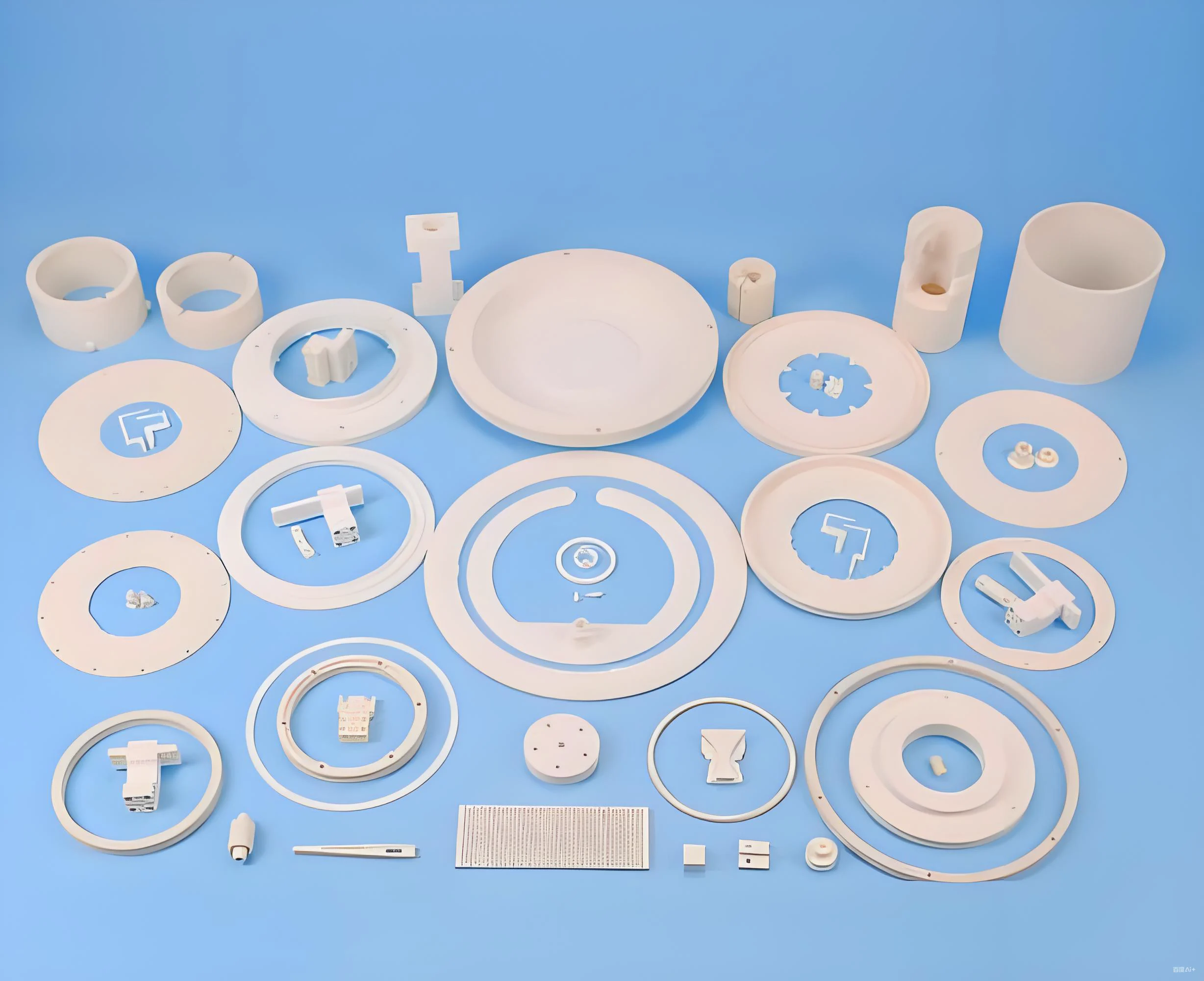
We specialize in OEM and custom ceramic components with over [10] years of experience in advanced ceramics. We offer fast prototyping, stable bulk supply, and full support from design to delivery. Our products comply with international quality standards and serve clients across Europe, North America, and Asia.